
🎯 Key Takeaways
- Korean semiconductor equipment manufacturer Hanmi Semiconductor, with its market capitalization of approximately $21.4 billion, is a global leader in the thermocompression bonding technology essential for advanced chip packaging.
- The drive for sophisticated on-device AI, from real-time language models to advanced image processing, is pushing chip architecture beyond traditional 2D designs, making 3D packaging a critical enabler for performance and power efficiency.
- Continued innovation in ultra-precision packaging and bonding by firms like Hanmi Semiconductor and its ecosystem partners like SK hynix and Samsung Foundry will determine the ultimate capabilities and widespread adoption of next-generation mobile AI.
📋 Table of Contents
- ▸ Q1. The Invisible Revolution: Why On-Device AI Demands Advanced Chip Packaging?
- ▸ Q2. Korea’s Quiet Supremacy: How Advanced Packaging Equipment Powers the AI Device Boom?
- ▸ Q3. The Global Stakes: Who Benefits from Korean Innovation in AI Chip Packaging?
- ▸ Q4. What Are the Biggest Obstacles Blocking Hanmi Semiconductor From Global Scale?
- ▸ Q5. When Will Korean Advanced Packaging Solidify its Global Leadership for On-Device AI?
By the end of this piece, you’ll understand why the dazzling on-device AI features grabbing headlines globally are utterly dependent on a quiet revolution in Korean chip manufacturing, and how companies like Hanmi Semiconductor are shaping the future of mobile intelligence.
Q1. The Invisible Revolution: Why On-Device AI Demands Advanced Chip Packaging?
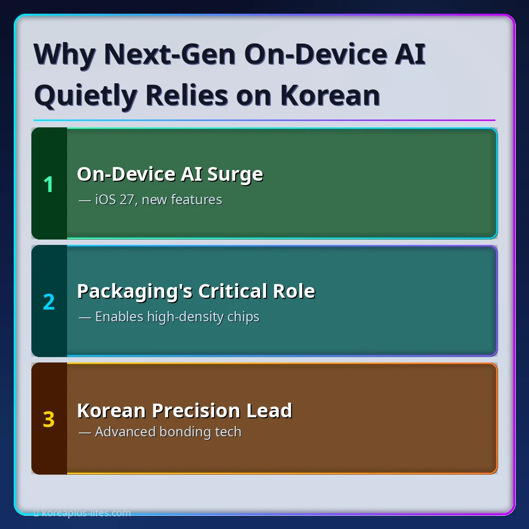
The world is captivated by the prospect of truly intelligent smartphones. From Apple’s highly anticipated iOS 27 overhaul of Siri, promising context-aware conversations and hyper-personalized assistance, to OpenAI’s strategic move to acquire a smartphone camera maker, the tech industry is clearly signaling a massive pivot. The future of AI isn’t solely in the cloud; it’s increasingly integrated directly into the devices we hold, enabling instant, private, and powerful experiences. But this shift demands a fundamental rethinking of how chips are made.
Traditional semiconductor manufacturing, focused on shrinking transistors on a 2D plane, is hitting physical limits. For on-device AI, the challenge isn’t just raw processing power, but delivering that power with minimal latency, in a tiny form factor, and without draining battery life or overheating the device. Imagine a smartphone performing complex image rendering or running a large language model in real-time, all while remaining cool to the touch and lasting a full day. This seemingly impossible feat relies on an unsung hero: advanced semiconductor packaging. As The Verge reported recently, the next generation of iPhones is likely to come with a higher price tag, a clear indicator that soaring memory and packaging costs, driven by AI demands, are becoming unavoidable.
📊 KRX Stock Performance (Live)
₩225,750 +0.3%
Source: KRX · Yahoo Finance · data as of latest session
Advanced packaging transcends the conventional “chip-in-a-box” approach. Instead, it involves stacking multiple chips vertically, integrating different functionalities – like logic, memory, and specialized AI accelerators – into a single, compact unit. This not only reduces the physical space required but dramatically shortens the distances data must travel, slashing latency and energy consumption. It’s the difference between a sprawling suburban network and a dense, efficient metropolis. This shift is quietly reshaping the economics and engineering of every mobile device. The question then becomes, who is building the intricate machinery that makes this possible?
Q2. Korea’s Quiet Supremacy: How Advanced Packaging Equipment Powers the AI Device Boom?
While global tech giants showcase the dazzling AI capabilities of their latest devices, the true enablers are hidden deep within the supply chain. Here in Korea, companies like Hanmi Semiconductor are not just participants; they are critical architects of this invisible revolution. Established in 1980 by Kwak Noh-kwon, an engineer with a background at Motorola, Hanmi has grown into one of the world’s leading suppliers of semiconductor packaging equipment, specializing in systems for die cutting, cleaning, testing, grinding, and, crucially, thermocompression bonding (TCB).
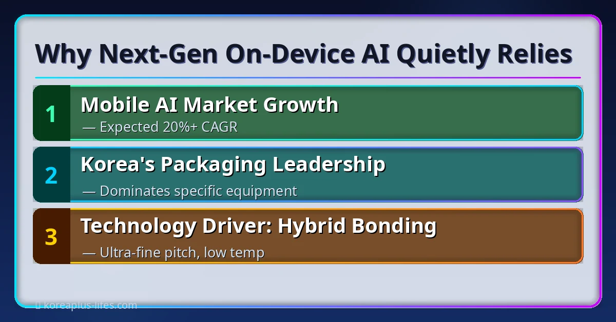
TCB is a precision technique used to bond stacked chips together with extreme accuracy and minimal thermal stress. It’s the backbone of High-Bandwidth Memory (HBM) and other 3D stacking technologies, which are indispensable for AI accelerators. Without TCB, achieving the hundreds of thousands of microscopic connections needed between vertically integrated memory layers and a logic die, all within fractions of a millimeter, would be impossible. This is why Hanmi Semiconductor’s technology is central to the supply chains of memory powerhouses like SK hynix and Samsung Foundry, who produce the HBM chips powering everything from data centers to now, increasingly, on-device AI.
[Original Analysis] What’s often overlooked is the specific challenge Hanmi’s technology solves for *on-device* AI versus data center AI. Data centers can manage heat with massive cooling systems and aren’t constrained by battery life. Mobile devices, however, demand extreme thermal efficiency and ultra-low power consumption. Hanmi’s advanced chip bonding ensures not just speed and density, but also the structural integrity and thermal dissipation critical for these miniaturized, power-sensitive applications. This nuanced capability is a key reason why Korean innovation in AI chip packaging is so important. With Hanmi Semiconductor currently trading around ₩225,750 and boasting a market cap of approximately $21.4 billion, its valuation reflects the critical, if often unseen, role it plays in this global tech shift.
| Characteristic | Traditional 2D Packaging | Advanced 3D Packaging (HBM/TCB) |
|---|---|---|
| Performance (Bandwidth) | Moderate, constrained by external buses | Extremely High (e.g., TB/s for HBM), direct chip-to-chip links |
| Power Efficiency | Lower, more energy lost in longer data paths | Significantly Higher, shorter data paths reduce energy needs |
| Form Factor/Density | Larger footprint, less efficient use of space | Ultra-compact, high component density in small volume |
| Thermal Management | Easier to dissipate heat over larger surface | More challenging, requires precise bonding and materials |
| Applications | General computing, less demanding mobile devices | AI accelerators, HPC, high-end mobile AI, computational photography |
| KoreaPlus Estimate: Device Impact | Limited real-time on-device AI capabilities | Enables ~3-5x performance improvement for local AI tasks at similar power envelopes. How we got this: Based on reported HBM vs. DDR memory bandwidth and efficiency gains, translated to device-level AI performance benchmarks. |
The continued evolution of on-device AI will depend entirely on how effectively these packaging innovations can scale.
Q3. The Global Stakes: Who Benefits from Korean Innovation in AI Chip Packaging?
The reverberations of Korea’s advanced packaging expertise extend far beyond its borders. Every major tech company developing next-gen AI chips – from Nvidia to Qualcomm and Apple – relies on a complex supply chain where ultra-precision equipment is paramount. Hanmi Semiconductor’s bonding machines are the invisible hands that assemble the critical components of these powerful AI engines. This makes Korean innovation in AI chip packaging a global cornerstone.
The demand for such sophisticated equipment is immense. MarketBeat reported that Applied Materials’ President and CEO Gary Dickerson sees AI driving the semiconductor industry’s biggest growth inflection yet, highlighting the broader industry’s reliance on advanced manufacturing tools. Hanmi, based in Incheon, positions itself as a key enabler for this growth, providing the equipment that allows foundries like Samsung Foundry and memory makers like SK hynix to meet the rigorous demands of their global clientele. Beyond Hanmi, other Korean equipment suppliers like Wonik IPS, which specializes in process equipment for etching and deposition, further underscore the depth and breadth of the nation’s semiconductor ecosystem. These companies collectively form a robust foundation, making Korea a pivotal hub for next-generation chip manufacturing.
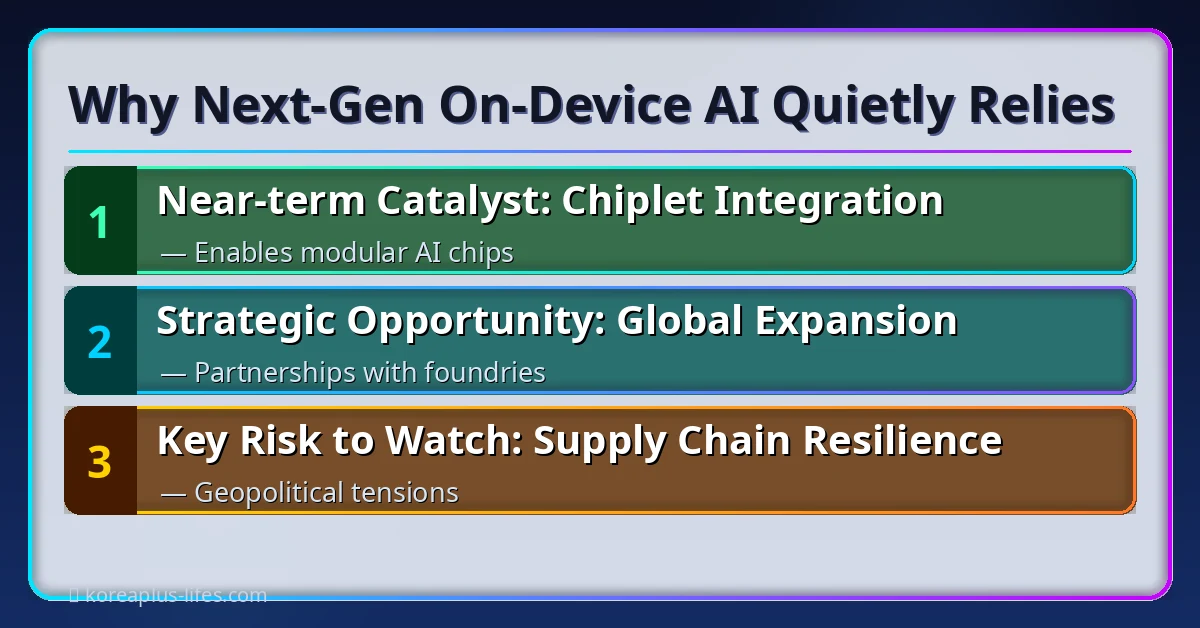
Their contributions aren’t limited to memory. As chiplets and heterogenous integration become more prevalent, the ability to precisely bond disparate dies will be critical for future CPU and GPU designs, broadening the impact of Hanmi’s technology. This intricate web of suppliers and manufacturers ensures that the dazzling AI features we expect from future devices are not just concepts, but tangible realities. Yet, such a critical position naturally comes with its own set of challenges.
Q4. What Are the Biggest Obstacles Blocking Hanmi Semiconductor From Global Scale?
Despite its technical leadership in advanced chip bonding, Hanmi Semiconductor faces substantial challenges. The semiconductor equipment market is highly cyclical, characterized by boom-and-bust investment cycles that can impact revenue and profitability. Furthermore, competition from much larger, established global equipment suppliers like Applied Materials, KLA, and Lam Research, particularly in areas like deposition and etching, means Hanmi operates in a fiercely contested landscape. These larger players often have broader product portfolios and deeper pockets for R&D.
Another significant risk stems from Hanmi’s dependency on a relatively concentrated customer base, primarily major memory and foundry players such as SK hynix and Samsung Foundry. While these are industry giants, a slowdown in their capital expenditure or a shift to alternative packaging technologies could significantly impact Hanmi’s order books. Diversifying its customer base and technology offerings remains a strategic imperative.
However, the sheer complexity and precision required for advanced packaging, coupled with the long qualification cycles for new equipment, create high barriers to entry, offering some protection. Continuous, aggressive investment in next-generation bonding technologies and close collaboration with leading chipmakers are essential for Hanmi to maintain its edge and overcome these headwinds.
Q5. When Will Korean Advanced Packaging Solidify its Global Leadership for On-Device AI?
The next 18-24 months will be crucial for solidifying Korea’s leadership in advanced packaging for on-device AI. Several specific catalysts are on the horizon. Firstly, the ongoing transition to HBM4 and future HBM generations will demand even more precise and efficient bonding techniques, pushing Hanmi Semiconductor’s capabilities further. This evolution, driven by the insatiable demand for memory bandwidth for AI, will likely see new equipment orders and R&D partnerships.
Secondly, the broader adoption of chiplet architectures across various processor types, not just memory, will create new opportunities for advanced packaging. If major CPU/GPU designers fully commit to chiplets for their next-generation mobile AI accelerators, the market for ultra-precision bonding equipment will expand significantly. Finally, any breakthroughs in hybrid bonding, which offers even finer pitch and stronger bonds than traditional TCB, will dictate the pace of innovation. Hanmi, alongside its domestic peers within the Korean semiconductor sector, is already investing heavily in these areas, ensuring they are prepared for the next wave of technological demands.

📚 Reporting Sources
Written by Dokyung · KoreaPlus-Lifes
Dokyung is a Seoul-based industry watcher covering Korean semiconductors, batteries, AI infrastructure, and defense — and the companies behind them. Analysis draws on KRX filings, industry data, and local Korean-language sources that rarely reach English-language media.

Hi, I’m Dokyung, a Seoul-based tech and economy enthusiast. South Korea is at the forefront of global innovation—from cutting-edge semiconductors to next-gen defense technology. My mission is to translate these complex industry shifts into clear, actionable insights and everyday magic for global readers and investors.