

🎯 Key Takeaways
- Hanmi Semiconductor’s thermal compression (TC) bonders are reportedly essential for manufacturing HBM, the advanced memory powering AI chips from companies like Nvidia.
- The company’s specialized equipment addresses a critical bottleneck in the advanced packaging process, ensuring the high-precision stacking required for AI accelerators.
- As global demand for AI chips continues to surge, Hanmi Semiconductor’s market position, reflected in its current stock price of ₩282,000, suggests sustained relevance in the coming years.
📋 Table of Contents
- ▸ From Early Vision to AI Dominance: Hanmi’s Packaging Journey
- └ The Origin Story
- └ The Turning Point
- ▸ A Critical Cog in the AI Machine: Hanmi’s Current Influence
- └ The Current State of Play
- └ Who’s Benefiting — and Who’s Not
- ▸ The Bottleneck Paradox: A Korean Advantage with Global Implications
- └ The Contradiction at the Heart of This Story
- └ Structural Challenges Going Forward
- ▸ The Next Five Years: Expanding Footholds in a Growing AI Landscape
- └ Common Questions
The race to build the world’s most powerful artificial intelligence chips is primarily a race for processing power, but it’s equally a contest for memory. Specifically, high-bandwidth memory, or HBM, has emerged as a non-negotiable component for feeding the hungry AI accelerators that power everything from data centers to advanced consumer electronics.
While industry giants like Nvidia design these chips and memory powerhouses such as SK hynix and Samsung Foundry produce the HBM modules, a crucial, often unseen, element of the global supply chain lies in South Korea: the specialized equipment required to package these intricate components. This is where Hanmi Semiconductor enters the picture, providing the sophisticated machinery that literally holds the AI revolution together.
From Early Vision to AI Dominance: Hanmi’s Packaging Journey
Hanmi Semiconductor is a South Korean firm specializing in semiconductor manufacturing equipment. Founded in 1980, the company initially focused on a range of general-purpose packaging and testing solutions for traditional semiconductors. Its early thesis centered on providing robust, precise equipment for a burgeoning global electronics industry, which was then transitioning from discrete components to integrated circuits.
The initial obstacle for many equipment makers, including Hanmi, was establishing credibility and precision against established Japanese and American competitors. However, the company steadily built a reputation for its lead cutting, molding, and vision placement equipment, laying the groundwork for more complex future applications. Its steady development in precision machinery meant it was positioned to adapt as packaging technologies evolved.
The Origin Story
Hanmi Semiconductor’s journey began with a focus on equipment for the back-end process of semiconductor manufacturing, a less glamorous but equally vital segment compared to front-end wafer fabrication. This included machines for sawing, cleaning, and testing, which are fundamental to preparing chips for integration into electronic devices. The company’s early investment in R&D, particularly in vision-based systems for precise component handling, distinguished it from many peers.
As the semiconductor industry matured, the need for advanced packaging methods to enable smaller, more powerful devices became apparent. Hanmi recognized this shift, gradually pivoting its expertise towards solutions for multi-chip integration. This foresight allowed it to build foundational technologies that would become critical for the era of stacked memory and chiplets, years before HBM became a mainstream requirement for AI. According to Wikipedia, Hanmi Semiconductor has consistently expanded its product portfolio to meet evolving industry needs, including thermal compression bonders, flip chip bonders, and saw & vision placement machines.
The Turning Point
The true turning point for Hanmi Semiconductor arrived with the advent of High-Bandwidth Memory (HBM). HBM modules consist of multiple layers of DRAM chips stacked vertically, interconnected by through-silicon vias (TSVs) to achieve unprecedented data transfer speeds. This intricate stacking process demands extreme precision and reliability, particularly in bonding the layers together.
Hanmi’s “Vision Placement & Thermal Compression Bonder” (TC Bonder) equipment became crucial for this process. Unlike traditional bonding methods, TC bonding uses heat and pressure to create highly reliable connections with minimal thermal stress, a necessity for the tightly packed HBM layers. This specialized equipment positioned Hanmi as a key enabler for HBM manufacturing, providing the tools that memory giants like SK hynix and Samsung Foundry require to produce next-generation memory. The decision to invest heavily in this niche, high-precision segment years ago now places Hanmi at the core of the global AI chip ecosystem.
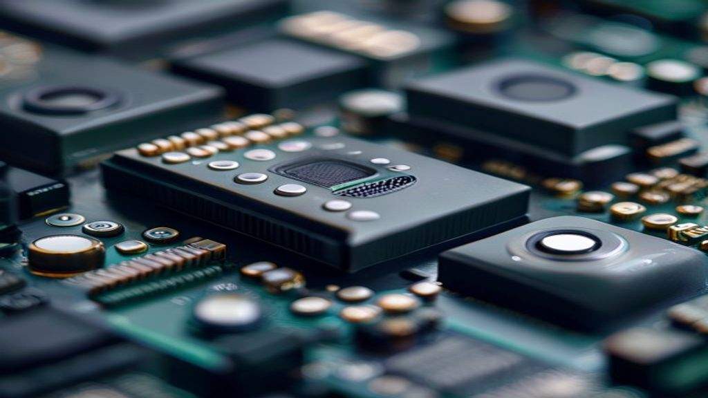
✦ AI-generated image for illustrative purposes
📊 KRX Stock Performance (Live)
₩282,000 -3.6%
Source: KRX · Yahoo Finance · data as of latest session
A Critical Cog in the AI Machine: Hanmi’s Current Influence
Hanmi Semiconductor currently holds a critical, if understated, position in the global AI chip supply chain. Its TC Bonders are highly sought after, with analysts estimating significant order backlogs as demand for HBM continues to outstrip supply. On May 30, 2026, Hanmi Semiconductor’s stock traded at ₩282,000, reflecting a market capitalization of approximately $26.7 billion, despite a 3.6% dip on the day. This valuation underscores investor recognition of its strategic importance, even if the general public remains largely unaware of its role.
The company’s advanced packaging equipment is not only used for stacking HBM but also for complex 2.5D and 3D integration processes, which are becoming standard for advanced AI accelerators. This broad utility extends its influence beyond just memory to the entire AI chip assembly process, making it a critical partner for leading foundries and chip designers. For a deeper understanding of this interdependence, see our analysis on Why AI Chip Manufacturing Depends on Companies Nobody Has Heard Of.
The Current State of Play
As of mid-2026, the demand for high-performance AI chips, which rely heavily on HBM, continues its upward trajectory. Hanmi Semiconductor’s advanced equipment for HBM packaging is indispensable for companies like SK hynix, a primary supplier of HBM to Nvidia, and Samsung Foundry, which is expanding its own HBM production and advanced packaging services. This positions Hanmi as a bottleneck-reliever, enabling the production goals of the world’s leading AI hardware providers.
The complexity of HBM manufacturing means that only a handful of equipment suppliers can meet the stringent requirements for precision and throughput. Hanmi Semiconductor’s established expertise in thermal compression bonding for HBM stacking makes it a key player in this specialized niche, effectively providing the critical infrastructure for the global AI boom. Its sustained focus on this core technology has allowed it to capture a significant portion of this high-value market segment.
Who’s Benefiting — and Who’s Not
The primary beneficiaries of Hanmi Semiconductor’s advanced packaging equipment are the major memory producers like SK hynix and Samsung Foundry, along with AI chip designers such as Nvidia, who rely on a steady supply of high-quality HBM. These companies gain from the precision and efficiency Hanmi’s machines provide, allowing them to meet the escalating demand for powerful AI accelerators. The current global memory crunch, which is “killing the cheap smartphone” according to Davidoks.blog, further emphasizes the premium placed on advanced memory production, where Hanmi’s tools are critical.
Conversely, companies that lack access to such specialized equipment or those attempting to develop in-house alternatives may face significant delays and increased costs. The high barrier to entry for developing competitive TC bonding technology means that smaller players or new entrants into the advanced packaging space are at a disadvantage, further cementing the market leadership of a few specialized providers, including Hanmi. This dynamic creates a concentrated supply chain, which, while efficient for leading players, can also introduce vulnerabilities.

✦ AI-generated image for illustrative purposes
The Bottleneck Paradox: A Korean Advantage with Global Implications
The reliance on a few highly specialized equipment providers like Hanmi Semiconductor creates a paradox in the global AI supply chain. While these companies enable the rapid advancement of AI technology, they simultaneously represent a potential bottleneck. A disruption in their operations, or a sudden surge in demand that outpaces their production capacity, could have cascading effects throughout the entire AI industry, impacting everything from data center buildouts to the availability of consumer devices.
This dynamic presents both a significant advantage for Hanmi, solidifying its market position, and a potential vulnerability for the global ecosystem. The intellectual property associated with advanced packaging, particularly for HBM, is fiercely protected, and developing alternatives requires substantial investment and time. As Digitimes recently reported, “TSMC faces AI supply strain as Samsung, Intel, and Apple test foundry alternatives,” indicating that even major foundries are seeking to diversify and secure their supply chains for advanced components, including packaging.
The Contradiction at the Heart of This Story
The core contradiction lies in the global AI industry’s public focus on the headline-grabbing AI chip designers and memory manufacturers, while a vital, lesser-known Korean equipment maker silently underpins much of that innovation. The efficiency and scale of AI chip production are critically dependent on Hanmi Semiconductor’s specialized machines, yet this dependence remains largely unacknowledged outside of specific industry circles. This creates a situation where the most sophisticated technological advancements rely on a manufacturing step that is both indispensable and concentrated.
The tradeoff is clear: while hyper-specialization allows for unparalleled precision and performance, it also centralizes risk. The current AI boom, fueled by increasing demand for HBM and advanced packaging, amplifies both the strategic importance of companies like Hanmi and the potential fragility of a global supply chain heavily reliant on a few unique nodes. A procurement director at a major AI hardware firm would likely know Hanmi well, but the broader investment community often doesn’t.
Structural Challenges Going Forward
One structural challenge for Hanmi Semiconductor and the wider advanced packaging sector is the intense competition for talent in specialized engineering fields. Developing and maintaining leadership in cutting-edge equipment like TC Bonders requires continuous innovation and a highly skilled workforce, which is increasingly scarce globally. Another challenge lies in the rapid evolution of AI chip architectures; if a fundamentally different packaging approach gains traction, Hanmi will need to swiftly adapt its product roadmap to maintain its competitive edge.
Furthermore, the high capital expenditure cycles inherent in semiconductor manufacturing can create volatility. While demand is currently surging, a future slowdown in data center investments or a shift in AI development paradigms could impact order volumes. The ongoing US Fed Funds Rate of 3.64 also influences global investment in capital-intensive industries, potentially affecting long-term expansion plans for both Hanmi and its customers. For more on ensuring reliability in this space, consider our analysis of Nvidia’s AI Supply Chain vs Korea’s Chip Testers: Who Ensures AI Reliability?
The Next Five Years: Expanding Footholds in a Growing AI Landscape
Over the next five years, Hanmi Semiconductor is likely to solidify its position further as an indispensable provider of advanced packaging equipment. If the demand for HBM continues its current growth trajectory, driven by the proliferation of increasingly powerful AI models, expect Hanmi to expand its production capacity and potentially diversify its offerings to encompass other forms of 3D integration and chiplet technologies. This expansion will be critical for major memory and foundry players who are increasingly emphasizing vertically integrated or co-packaged solutions.
The company will need to navigate potential headwinds from rising competition in the broader packaging equipment space, as larger players like Applied Materials, which recently acquired NEXX, and Lam Research, touted as a top AI stock by Oppenheimer analysts in April 2026, also expand their advanced packaging portfolios. However, Hanmi’s highly specialized focus on critical HBM bonding processes provides a distinct advantage. Its ability to iterate quickly and maintain a technological lead in this specific niche will determine its trajectory. Continued investment in R&D and strategic collaborations within the Korean semiconductor ecosystem will be key to sustaining its growth.
Common Questions
A1. Korean companies are crucial for AI chip manufacturing due to their dominance in high-bandwidth memory (HBM) production and advanced packaging equipment. Companies like SK hynix and Samsung Foundry are leading HBM development, while specialized firms such as Hanmi Semiconductor provide the essential machinery for assembling these complex components. This integrated ecosystem allows for rapid innovation and efficient scale in a critical segment of the global AI supply chain. For more on Korea’s role, explore our K-Tech & Gadgets category.
A2. Hanmi Semiconductor contributes to AI chips by supplying advanced packaging and testing equipment, most notably its thermal compression (TC) bonders. These machines are essential for precisely stacking the multiple layers of high-bandwidth memory (HBM) required for AI accelerators. Without Hanmi’s specialized solutions, the intricate manufacturing processes for integrating HBM with logic chips would be significantly hampered, making the company a silent enabler of the AI boom since its critical equipment facilitates the complex assembly steps.

Hi, I’m Dokyung, a Seoul-based tech and economy enthusiast. South Korea is at the forefront of global innovation—from cutting-edge semiconductors to next-gen defense technology. My mission is to translate these complex industry shifts into clear, actionable insights and everyday magic for global readers and investors.