Samsung’s HBM Lag: Why the Tech Giant Lost Round One to SK Hynix (And Its HBM4 Plan to Win the War)

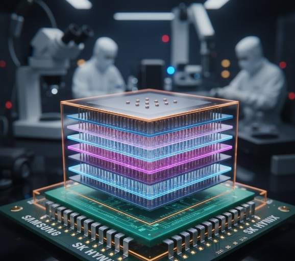
A vibrant, glowing HBM (High Bandwidth Memory) chip stack with multiple layers, resting on a circuit board. The background shows blurred cleanroom engineers and lab equipment, symbolizing advanced semiconductor manufacturing. The chip base is labeled "SAMSUNG" and "SK HYNIX."

The HBM War: SK Hynix Won the Battle, Samsung Plans to Win the War The global AI revolution runs on High Bandwidth Memory (HBM). In the critical battle for HBM3E, SK Hynix has secured a decisive—and, to many, surprising—lead, appearing to dethrone the long-reigning champion, Samsung. However, from a perspective on the ground in Seoul, … 더 읽기

Revolutionizing Mobile Technology: SK Hynix and the Future of On-Device AI

SK Hynix,On-Device AI,ZUFS 4.0,Korea

Developing a Market-Leading Technology SK Hynix announced on May 9, the successful development of ZUFS 4.0, a mobile NAND solution optimized for smartphones. This technology, an evolution of Universal Flash Storage (UFS), incorporates zoned-storage capabilities, allowing data to be stored in specific zones based on frequency of use and type. Such segmentation significantly enhances the … 더 읽기

SK Hynix’s $15 Billion Investment in Cheongju: Driving AI Memory Leadership

SK Hynix,Cheongju,fab plant,ai memory,Vision

Preparing for the AI-Driven Future On April 24th, SK Hynix disclosed their decision following a board resolution to construct the new Fab M15X facility in Cheongju, North Chungcheong Province. This initiative reflects their proactive approach to meeting the explosive demand for AI semiconductors. The initial phase involves an investment of 5.3 trillion KRW to commence … 더 읽기