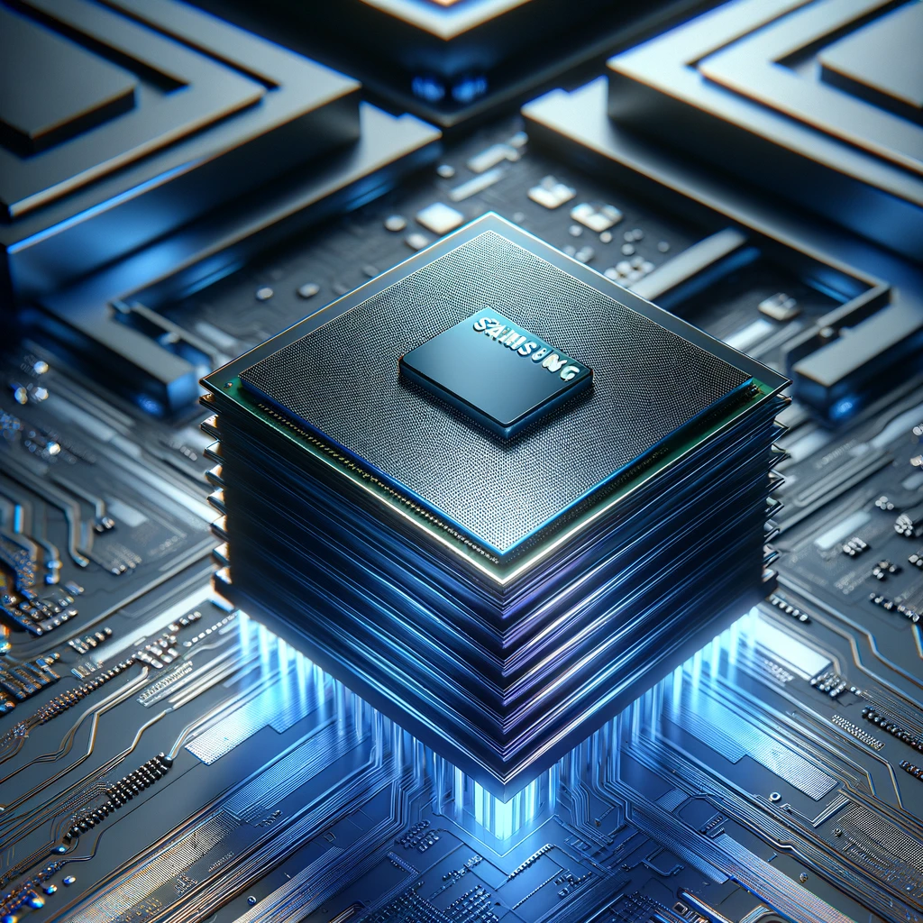
Samsung’s HBM Lag: Why the Tech Giant Lost Round One to SK Hynix (And Its HBM4 Plan to Win the War)

A vibrant, glowing HBM (High Bandwidth Memory) chip stack with multiple layers, resting on a circuit board. The background shows blurred cleanroom engineers and lab equipment, symbolizing advanced semiconductor manufacturing. The chip base is labeled "SAMSUNG" and "SK HYNIX."

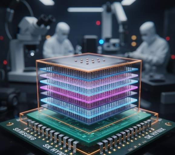
The HBM War: SK Hynix Won the Battle, Samsung Plans to Win the War The global AI revolution runs on High Bandwidth Memory (HBM). In the critical battle for HBM3E, SK Hynix has secured a decisive—and, to many, surprising—lead, appearing to dethrone the long-reigning champion, Samsung. However, from a perspective on the ground in Seoul, … 더 읽기

Samsung Electronics Appoints New Head of Semiconductor Division Amid Strategic Overhaul

Samsung,Semiconductor,Strategic,Innovation

Samsung Electronics has recently made a significant change in its leadership, appointing Young-Hyun Jun as the new head of its Device Solutions (DS) division. This strategic move comes in the wake of substantial financial losses in the semiconductor sector, aiming to rejuvenate the company’s approach and enhance its future competitiveness. In the past year, Samsung’s … 더 읽기

Samsung to Launch Next-Generation 16-Layer High Bandwidth Memory in the Coming Year

Samsung,memory,capacity,speed,hbm4,speed

During an interview with Samsung’s Semiconductor Newsroom on April 18, Yun Jae-yun, Executive Vice President of DRAM Development at Samsung Electronics, announced the company’s adoption of advanced Non-Conductive Film (NCF) assembly technology, which is optimized for high-temperature thermal characteristics. This breakthrough will be integral to their next-gen HBM4, employing a 16-layer stack technology, referred to … 더 읽기